New DRAM value‑per‑area chart draws attention amid rising memory prices
Source ↗
👁 0
💬 0
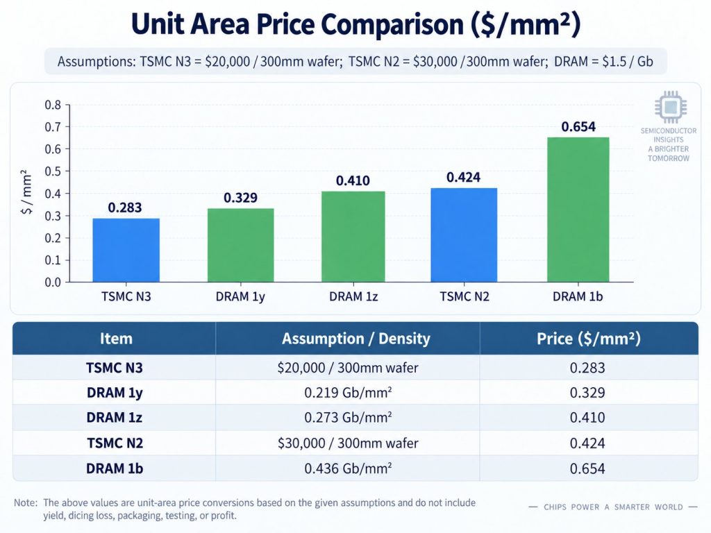
A new DRAM wafer‑value comparison has been making the rounds this week, illustrating how current memory pricing places modern DRAM generations above leading‑edge logic nodes on a per‑mm² basis.
The chart originates from Kurnal, who converted DRAM bit density and spot‑price assumptions into a simple “value per square millimetre” comparison. The graphic compares several DRAM generations against nominal per‑mm² wafer pricing estimates for TSMC’s N3 and N2 logic processes.
Image credit: Kurnal
Tom’
The chart originates from Kurnal, who converted DRAM bit density and spot‑price assumptions into a simple “value per square millimetre” comparison. The graphic compares several DRAM generations against nominal per‑mm² wafer pricing estimates for TSMC’s N3 and N2 logic processes.
Image credit: Kurnal
Tom’


Comments (0)